The Strand Campus is home to a range of High-performance imaging equipment. The basement of the King’s building is home to two Electron Microscopes. The Zeiss EVO is equipped with and energy dispersive spectroscopy (EDS) detector and the TESCAN Mira 3 is equipped with a Cathodoluminescence spectrometer. The Strand building houses two atomic force microscopes.
For more information, please contact:
Dr. Feng Wang: Technical Manager (Electron Microscopy) - feng.wang@kcl.ac.uk
Ben Blackburn: Senior Technical Manager (Operations) – ben.blackburn@kcl.ac.uk
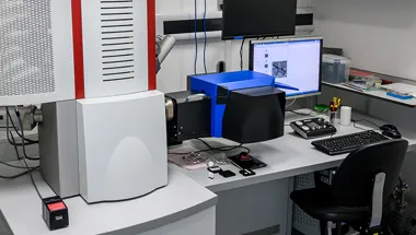
Scanning Electron Microscopy
Unlike light microscopy, scanning electron microscopy (SEM) produces images of a sample by bombarding them with a fine electron beam and recording the verious interactions of the electrons with the sample surface. SEMs consist of a probe that acts as an electron source. These are typically constructed of tungsten or Lanthanum hexaboride. The electron beam is focussed and manipulated using an array of electro-optical lenses in the SEM column, before contacting the sample. The beam scans the sample surface in a mulit-directional raster scan. Electrons that are emmitted/ scattered by the sample are picked up by various detectors and used to construct a highly detailed image.
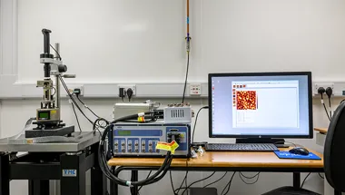
Atomic Force Microscopy
Atomic Force Microscopy (AFM) is a high-resolution non-optical imaging technique. Rather than imaggin by bombarding with photons or electrons, direct topographical information is obtained by moving an atomically sharp AFM tip over a sample surface. The AFM tip is positioned at the end of a flexible probe cantilever. As the tip is dragged over the surface, it is defected by the topographical features, which in turn move the cantilever in the z direction. A laser beam is used to track the surface defection and this is combined the x and y coordinates of the scan to construct three dimensional maps of the sample surface.
Scanning electron microscopy and atomic force microscopy
Related equipment
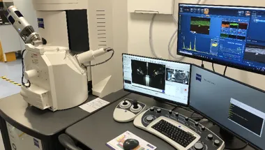
Zeiss EVO LS15 ESEM
ESEM with EDS analysis
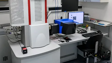
Tescan Mira 3 with Delmic SPARC Cathodoluminescence Detector
FEG-SEM with Cathodoluminescence Detector
Bruker Dimension ICON Atomic Force Microscope
AFM with tapping, resonance and contact modes for topographical and conductivity analysis
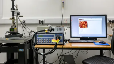
Bruker MultiMode 8 Atomic Force Microscope
Bruker MultiMode 8 Atomic Force Microscope

Scanning Electron Microscopy
Unlike light microscopy, scanning electron microscopy (SEM) produces images of a sample by bombarding them with a fine electron beam and recording the verious interactions of the electrons with the sample surface. SEMs consist of a probe that acts as an electron source. These are typically constructed of tungsten or Lanthanum hexaboride. The electron beam is focussed and manipulated using an array of electro-optical lenses in the SEM column, before contacting the sample. The beam scans the sample surface in a mulit-directional raster scan. Electrons that are emmitted/ scattered by the sample are picked up by various detectors and used to construct a highly detailed image.

Atomic Force Microscopy
Atomic Force Microscopy (AFM) is a high-resolution non-optical imaging technique. Rather than imaggin by bombarding with photons or electrons, direct topographical information is obtained by moving an atomically sharp AFM tip over a sample surface. The AFM tip is positioned at the end of a flexible probe cantilever. As the tip is dragged over the surface, it is defected by the topographical features, which in turn move the cantilever in the z direction. A laser beam is used to track the surface defection and this is combined the x and y coordinates of the scan to construct three dimensional maps of the sample surface.
Facility staff
Scanning electron microscopy and atomic force microscopy
Related equipment

Zeiss EVO LS15 ESEM
ESEM with EDS analysis

Tescan Mira 3 with Delmic SPARC Cathodoluminescence Detector
FEG-SEM with Cathodoluminescence Detector
Bruker Dimension ICON Atomic Force Microscope
AFM with tapping, resonance and contact modes for topographical and conductivity analysis

Bruker MultiMode 8 Atomic Force Microscope
Bruker MultiMode 8 Atomic Force Microscope

