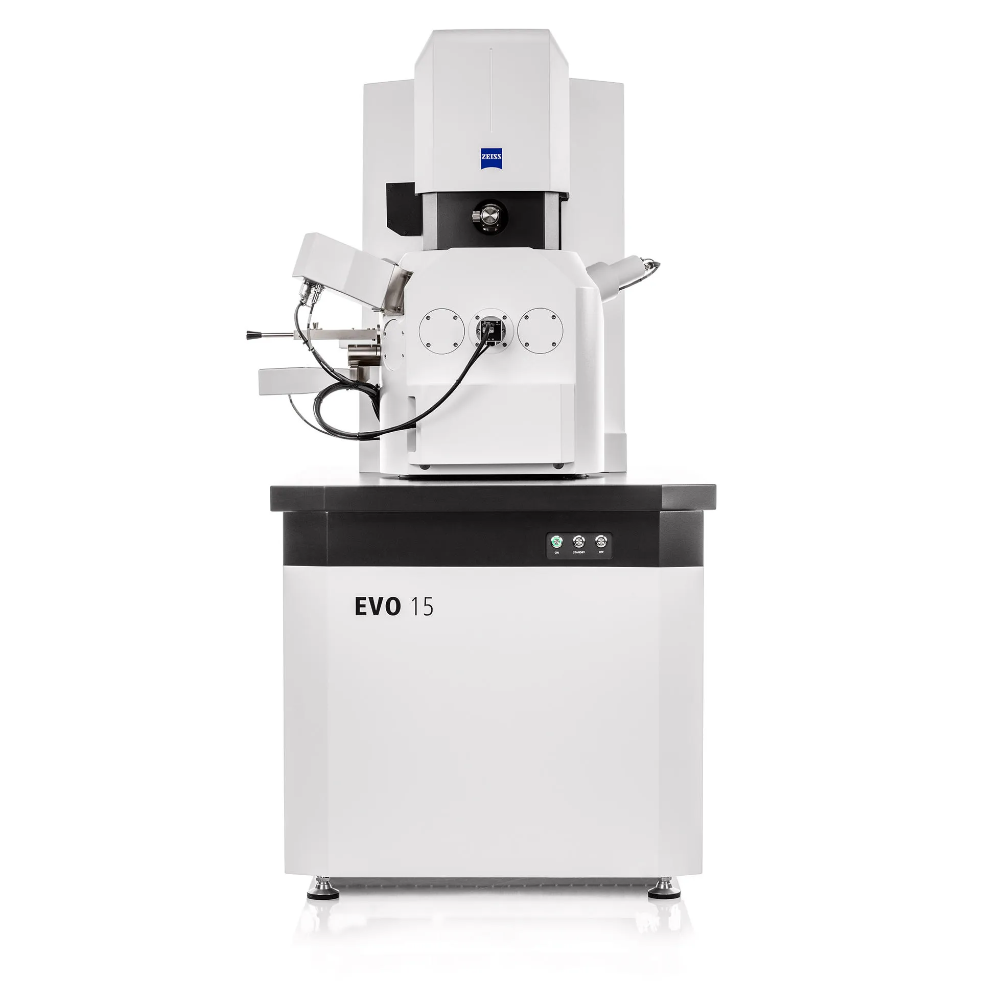
Take Your Investigation to the Next Level.
The EVO LS15 SEM takes over when you’ve reached the resolution or contrast limit of light microscopy, but still need answers.
High Resolution Surface Morphology
Secondary electron (SE) imaging –with a maximum resolution of a couple of nanometers – comfortably covers most of the sub-micron length-scale. While light microscopy yields contrast(reflections) from surfaces, secondary electron emission yields contrast from edges on the sample surface, thereby providing greater detail of surface morphology, such as that of metal fractures.
Compositional Imaging
Backscattered electron (BSE) imaging yields contrast that is directly proportional to the density of the materials that constitute your parts or assemblies. It provides a snapshot of compositional heterogeneity that can help you determine the root cause of material failure or quality excursions.
ZEISS Smart EDX
If SEM imaging alone isn’t enough to gain a complete understanding of parts or samples, investigators will turn to Energy Dispersive Spectroscopy (EDS) to acquire spatially resolved elemental information from these surfaces.
ZEISS Smart EDX is the dedicated microanalysis solution designed specifically for analytical routine applications performed on the ZEISS EVO to improve both ease of use and workflow repeatability in multi-user environments.


Contact us
For more information about the London Centre for Nanotechnology at King's, please contact us at:
